Power Supply Module 1.1 and 1.2 for Series 1 FPGA Boards
Series 1 FPGA Boards are deprecated. Please switch to Series 2.
An Adapter is available as workaround.
The old product page is still available here for documentation purposes.
|
Features Additional resources
Schematics of Power Supply Module 1.1 (PDF) |
 |
Features
- Power supply board for USB-FPGA Modules 1.2, 1.11 and 1.15.
- High-efficiency switching regulators to generate the supply voltages:
Voltage Current Power Supply Module 1.1 Power Supply Module 1.2 1.2V 8 A 2 A 2.6 V 2.5 A 2 A 3.3 V 2.5 A 2 A - I/O voltages VCCO_RIGHT / VCCO_IO and VCCO_TOP can be easily and independently set to 3.3V, 2.6V, 1.2V or to an external voltage.
- JTAG interface for the FPGA
Functional description
The following drawing shows the measurements and the location of the of the described elements.
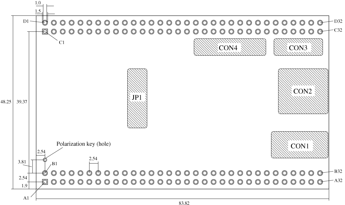
Click on the image for a larger version or download the PDF version.
External power: CON1 and CON2
CON1 is a standard DC power jack with 2.1mm center pin diameter for a supply voltage of 4.5 V to 16 V. The DC connector delivered with the Power Supply Module can be installed on both sides.Alternatively CON2 can be used to connect non standard power cables. The ground pin of CON2 (round pad) is marked with "-" and the supply pin (quadratic pad) is marked with "+", see the images below. The connector set delivered with the board can be installed on both sides.
If non-stabilized power supplies are used it must be made sure that the peak voltage is not larger then 18V.
Hints for power supply via USB can be found on the ZTEX Wiki.
JTAG connector: CON4, CON3
The Power Supply Module contains two JTAG connectors. CON3 is a 14 pin, 2.0mm pitch connector standardized by Xilinx. installed on the bottom side.CON4 can be used to connect non-standard JTAG programmers. If used, the pin header delivered with the board has to be
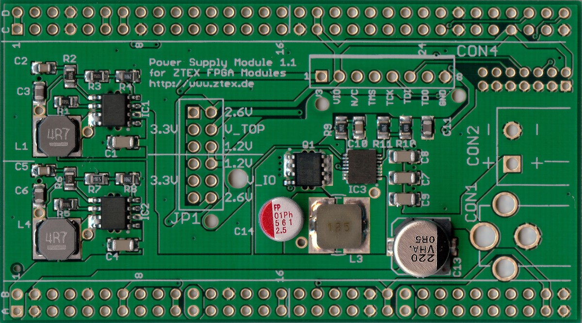
The pin descriptions can be found in the silk screen (see the images).
The voltage for the I/O signals (TCK,TMS,TDI,TDO) is 2.6V. The supply pin of this voltage is labelled with "VIO". The "3V3" pin to CON7 can be used as 3.3V supply for the JTAG adapter.
I/O voltages: JP1
Jumper JP1 sets the I/O VCCO_IO(=VCCO_RIGHT) and VCCO_TOP, respectively. A pin header is delivered with the board and can be installed on both sides.On Spartan 6 USB-FPGA Modules 1.11 and 1.15 V_TOP has no function. (The I/O voltage of the pins at rows C,D and F of the I/O Connector is fixed to 3.3V.)
By closing this jumpers (see images below) the I/O voltages can be switched easily to 3.3V, 2.6V or 1.2V. If other I/O voltages are required the jumpers must be left open and the I/O voltage must be supplied via the pins of the I/O Connector.
[TOC]
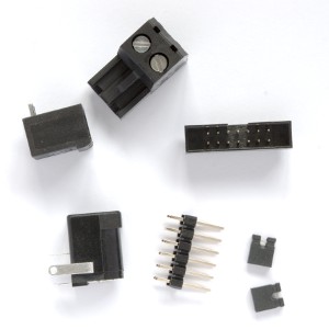
Package contents
|
|
Images
Click on the images for larger pictures.
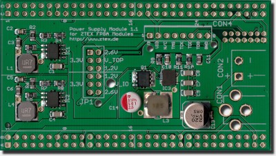
Top side of the Power Supply Module 1.1. |
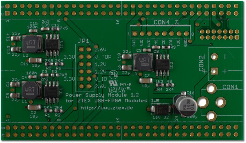
Top side of the Power Supply Module 1.2. |
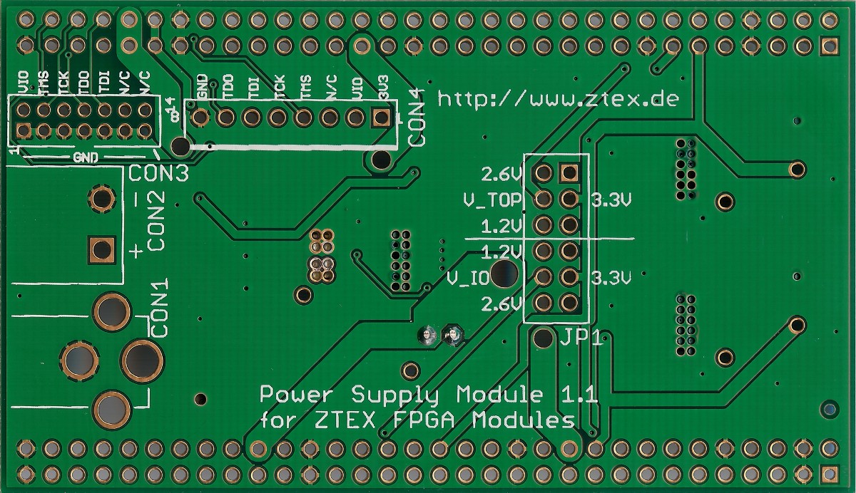
Bottom side of the Power Supply Module 1.1. |
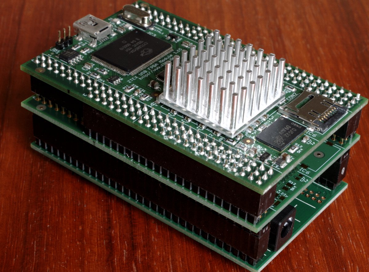
Typical application configuration: Spartan 6 LX45 to LX150 USB-FPGA Module 1.15 stacked on a application circuit and a Power Supply Module 1.1.
|