USB-FPGA Module 1.15y:
Quad-Spartan 6 LX150 FPGA Board with USB 2.0 Microcontroller
USB-FPGA Modules 1.15y are deprecated. Please switch to Series 2 FPGA Boards.
The old product page is still available here for documentation purposes.
|
The USB-FPGA Module 1.15y contains four Spartan 6 XC6SLX150 FPGA's, on-board voltage regulators and a USB controller. It is optimized for computations that do not require much bandwidth and RAM. The FPGA Board allows to build large low-cost clusters using standard components.
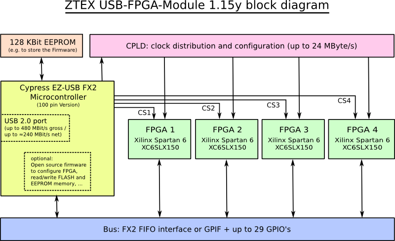
Block diagram
Schematics (rev. 1, PDF) |
 |
Block diagram
Features
- Four Xilinx Spartan 6 FPGA LX150 (XC6SLX150) FPGA, speed grade 3N
- High-Speed (480 MBit/s) USB interface via Mini-USB connector (B-type)
- Cypress CY7C68013A EZ-USB FX2 Microcontroller
- 128 Kbit EEPROM memory (can be used to store the EZ-USB firmware)
- 2 Kbit MAC-EEPROM: contains a unique non erasable MAC-address
- High efficiency on-board power supply:
- Wide input range: 4.5 V to 16 V
- 3.3 V @ 1.5 A
- 4 x 1.2 V @ 8A
- On-Board temperature sensors (since Rev. 2)
- Large heat sinks for active or passive cooling
- Fast FPGA configuration using CPLD: 24 MByte/s via USB
- FPGA configuration / programming via USB using the free SDK. (No JTAG adapters or other additional utilities required.)
- Non-free Xilinx ISE License or an Evaluation License required for FPGA development
Applications
The FPGA Board is optimized for computations that do not require a much bandwidth and RAM such as:- Bitcoin-Mining
- Monte Carlo methods
- Computation of Rainbow Tables
- Brute-force searches
- Bioinformatic calculations
SDK, Examples, Getting Started
A powerful open source Firmware Development Kit with platform independent host software API is available for the FPGA Board. This SDK allows to define all USB device descriptors using only a few macro commands, and thus gives the developer a quick start into Firmware programming.The SDK package contains a lot of examples which can be used as starting point for own applications.
More Information are available in the EZ-USB FX2 SDK section.
Additional documentation including Tutorials can also be found on the ZTEX Wiki
Functional description
The following drawing shows the measurements and the location of the of the described elements.
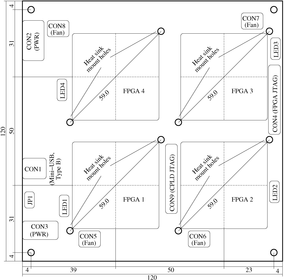
Click on the image for a larger version or download the PDF version.
FPGA configuration
There are two ways to configure the FPGA:- From USB with the SDK. This can be done using the API (see configureFpga) or using the utilities FWLoader or DeviceServer. DeviceServer allows comfortable access to the FPGA Board using the http interface and your Web browser as GUI.
- Via JTAG, see JTAG section below. Bitstream upload to large FPGA's (like XC6SLX150) via JTAG may take quite long. Therefore the USB method should be preferred.
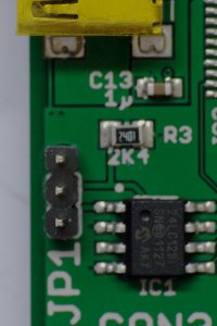
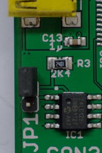
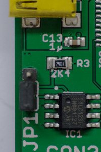
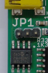
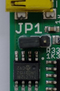
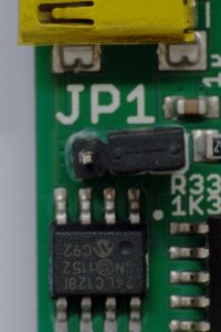
EEPROM address: JP1
Jumper JP1 specifies the I2C address of the EEPROM:
| JP1 | I2C address |
| open | 0xA2 |
| close | 0xAA |
The EZ-USB FX2 Microcontroller searches for the firmware at the address 0xA2 which is the default address (jumper open).
The main purpose of this jumper is to disable boot-loading from EEPROM. If, for example, the EEPROM was programmed with a corrupt firmware the Microcontroller can be booted with the internal firmware by closing JP1 during powering-on.
JP1 has an unconnected pin which can be used for parking the jumper. The following pictures show all possible jumper positions:
|
|
| Rev. 1: JP1 open | Rev. 1: JP1 closed |
|
|
| Rev. 2: JP1 open | Rev. 2: JP1 closed |
FPGA state: LED1-LED4
LED1-LED4 indicates the configuration state of the FPGA's as follows:
| LED<n> | FPGA<n> |
| on | unconfigured |
| off | configured |
External power: CON2 and CON3
CON3 is a standard DC power jack with 2.1mm center pin (+) diameter and 5.5mm barrel (-) diameter for a supply voltage of 4.5 V to 16 V.CON2 is a pluggable terminal. The two outer contacts are GND (-) and the inner contact is the supply voltage (+). This connector is designed for large currents and should therefore be preferred. The terminal block is delivered with the board.
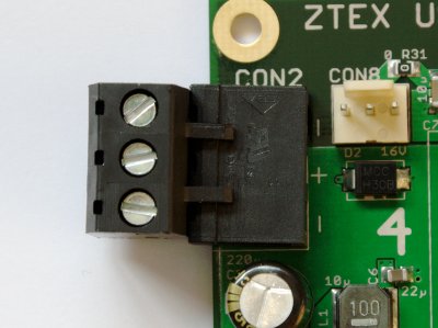
If non-stabilized power supplies are used it must be made sure that the peak voltage is not larger then 16V, see also Power supply selection guide on the Wiki.
Suggestions for the power supply of FPGA clusters are on the FPGA cluster power supplies page on the Wiki.
Configuration booster and clock distribution CPLD
The CPLD boosts the configuration speed the FPGA to about 24 MByte/s and distributes the clock signals. A block diagram which depicts the CPLD operation is depicted below.
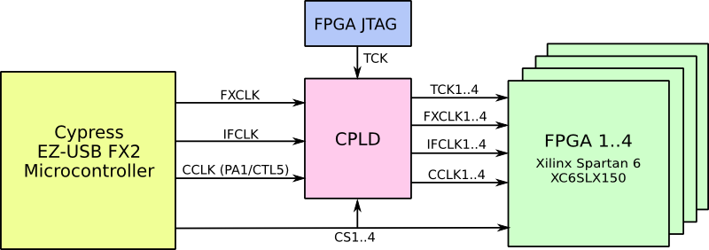
The high speed configuration mode requires an output Endpoint of the EZ-USB FX2. The Firmware allows to (re-)use an endpoint which is intended for user defined communication. If all Endpoint buffers of the EZ-USB FX2 are required for input Endpoints standard speed (about 1 MByte/s) configuration via Endpoint 0 has to be used.
The CPLD is factory programmed. Re-programming via JTAG is possible. The sources files and jed file can be downloaded here: usb-fpga-1.15-cpld.zip.
FPGA-JTAG (CON4)
The FPGA can be configured either via USB or via JTAG. If the JTAG interface is used for FPGA configuration bit 0-3 of port E (=PROG_B at FPGA's 1-4) must be driven high. This happens automatically if a firmware developed with the SDK is running.
The FPGA JTAG connector CON4 is not installed by default. It is delivered with the board on request.
Clock resources
On the FPGA board two clocks sources are available: the clock output of the EZ-USB FX2 which is usually configured to 48 MHz and the interface clock which can be configured to 30 MHz or to 48 MHz. They can be used to generate new clocks within the FPGA using DCM's or PLL's.The clock signal are distributed using the CPLD.
Heat Sinks
For high performance / high speed applications heat sinks are required. USB-FPGA Modules 1.15y are prepared for large standard heat sinks (up to 40 mm x 40 mm) with push pins and a hole distance of 59mm. If the input voltage is 12V CON5-CON8 can be used to connect fans.Four Xilence COO-XPNB.F heat sinks are delivered with the board. These heat sinks can be used actively or passively. In passive mode the fan should be removed. The height of the heat sink (without fan) is 35 mm. The height of the fan is 11 mm.
In order to ensure sufficient heat transfer the heat sinks has to be mounted using the push pins and thermal grease.
If a low profile cooling solution is required Titan TTC-CSC03 coolers are recommended.
List of Connections
A List of Connections can be downloaded in Gnumeric and Excel format.
Images
Click on the images for larger versions.
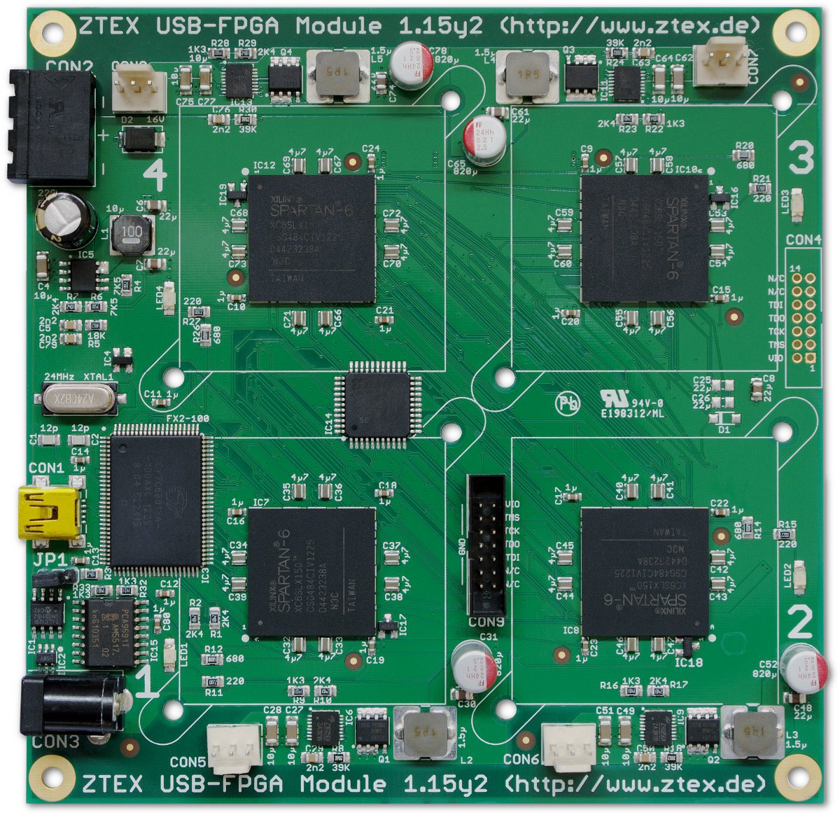
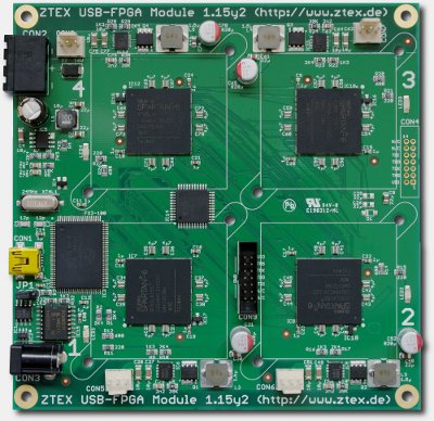
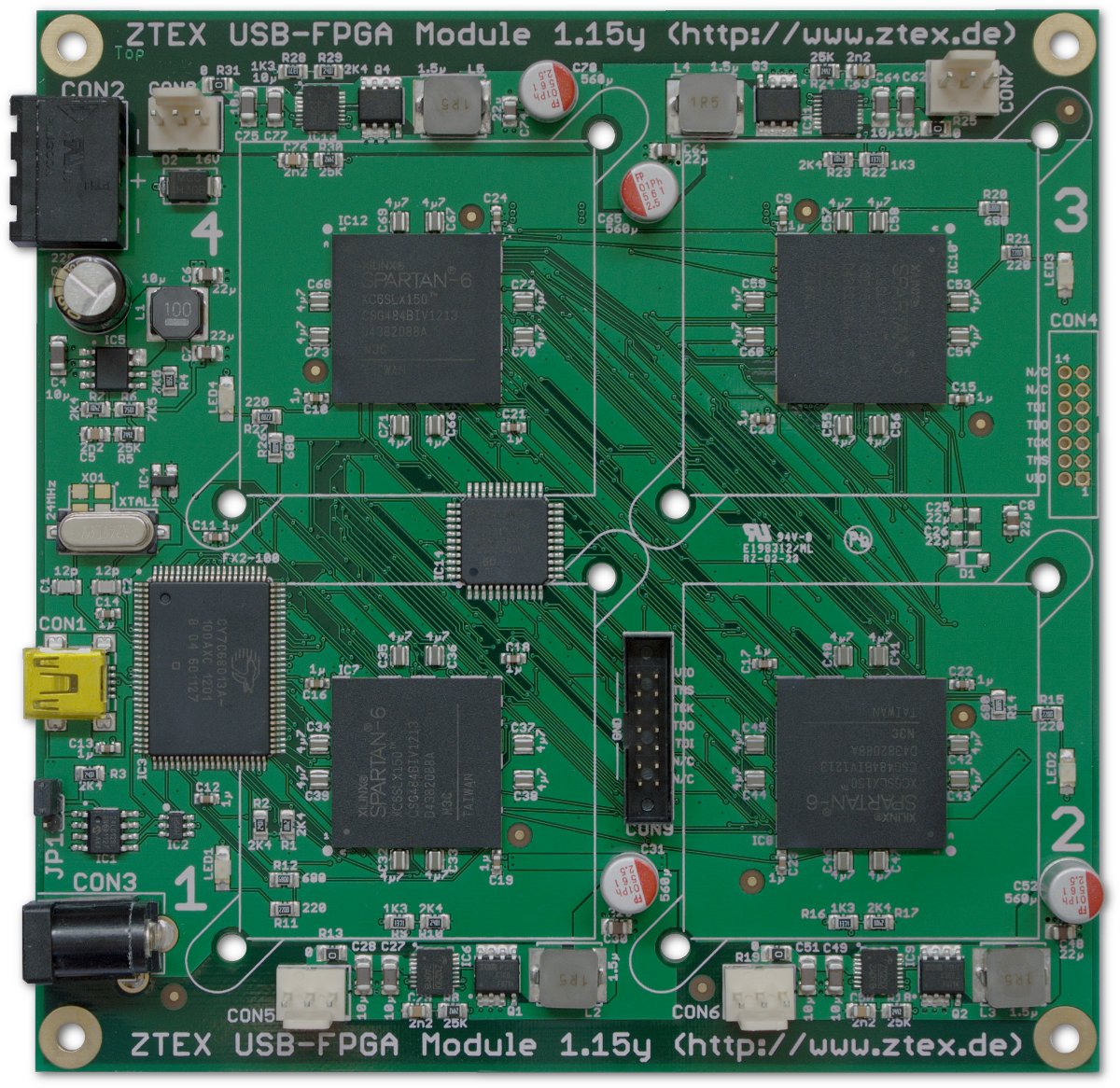
USB-FPGA Module 1.15y, rev. 2 without heat sinks. This Spartan 6 LX150 (XC6SLX150) Quad-FPGA Board is optimized for cryptographic computations and allows to build low-cost clusters using standard components. |
USB-FPGA Module 1.15y, rev. 1 without heat sinks. This Spartan 6 LX150 (XC6SLX150) Quad-FPGA Board is optimized for cryptographic computations and allows to build low-cost clusters using standard components. |
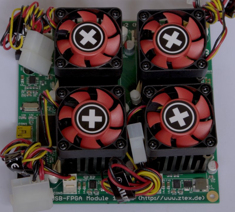
USB-FPGA Module 1.15y with installed heat sinks. The heat sinks are delivered with the board. This FPGA Board contains four Spartan 6 LX150 (XC6SLX150) FPGA and is suitable for cryptographic computations such as Bitcoin Mining. |